當前位置:首頁 > 産品中(zhōng)心 > 二維材料 > 二維材料薄膜 > 基于藍(lán)寶石襯底的全區域覆蓋的單層二硒化铼

相關文章
Related Articles詳細介紹
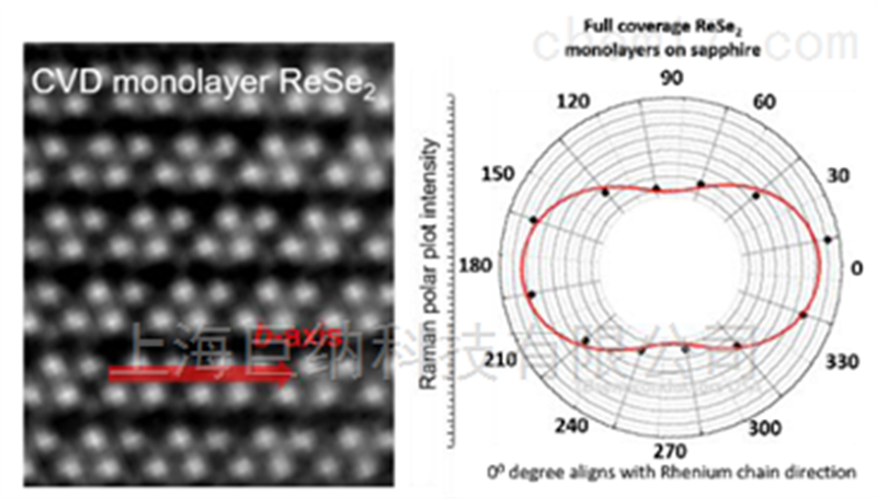
This product contains full area coverage ReSe2 monolayers on c-cut sapphire substrates. Sample size measures 1cm in size and the entire sample surface contains monolayer thick ReSe2 sheet. Synthesized full area coverage monolayer ReSe2 is highly crystalline, some regions also display significant crystalline anisotropy.
Sample Properties.
Sample size | 1cm x 1cm square shaped |
Substrate type | Sapphire c-cut (0001) |
Coverage | Full monolayer coverage |
Electrical properties | 1.45 eV Anisotropic Semiconductor (Indirect Bandgap) |
Crystal structure | Distorted Tetragonal Phase (1T’) |
Unit cell parameters | a = 0.656 nm, b = 0.672 nm, c = 0.674 nm, α = 91.74°, β = 105°, γ = 119° |
Production method | Atmospheric Pressure Chemical Vapor Deposition (APCVD) |
Characterization methods | Raman, angle resolved Raman spectroscopy, photoluminescence, absorption spectroscopy TEM, EDS |
Specifications
ReSe2 monolayers do not contain intentional dopants or defects. However, our technical staff can produce defected ReSe2 using α-bombardment technique.
Supporting datasets [for 100% Full area ReSe2 monolayers on c-cut Sapphire]
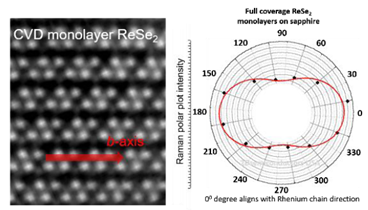
Transmission electron images (TEM) and angle resolved Raman spectroscopy measurements acquired from CVD grown full area coverage ReSe2 monolayers on c-cut sapphire confirming crystalline anisotropy
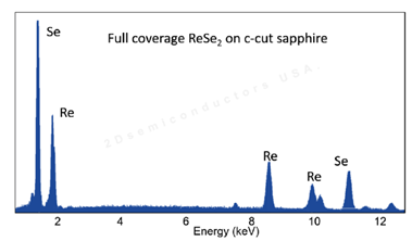
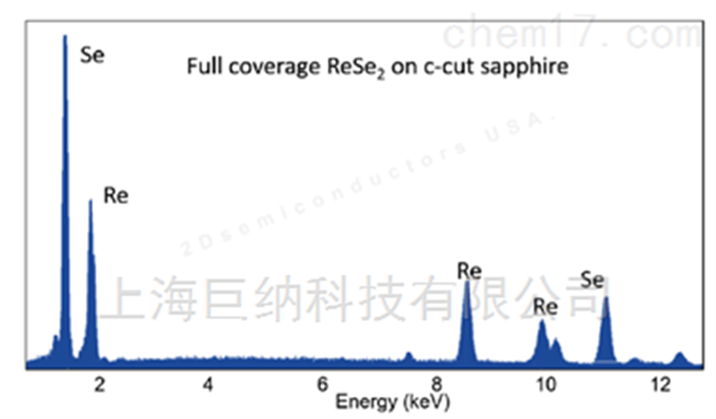
Energy dispersive X-ray spectroscopy (EDX) characterization on CVD grown full area coverage monolayer ReSe2 on c-cut sapphire
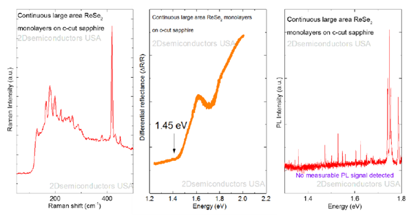
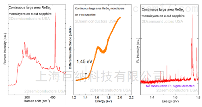
Raman spectroscopy measurement confirm monolayer nature of the CVD grown samples. Differential reflectance measurements clearly show band gap at 1.45 eV for monolayer ReS2 consistent with the existing literature values. PL spectrum does not show any PL signal due to indirect band nature.
産品咨詢
聯系我(wǒ)們
上海逅飛科技有限公司 公司地址:上海市虹口區寶山路778号海倫國際大(dà)廈5樓 技術支持:化工(gōng)儀器網掃一(yī)掃 更多精彩

微信二維碼

網站二維碼
微信掃一(yī)掃
