當前位置:首頁 > 産品中(zhōng)心 > 二維材料 > 二維材料薄膜 > 基于藍(lán)寶石襯底的全區域覆蓋的單層二硫化鎢

相關文章
Related Articles詳細介紹
This product contains full area coverage WS2 monolayers on c-cut sapphire substrates. Sample size measures 1cm in size and the entire sample surface contains monolayer thick WS2 sheet. Synthesized full area coverage monolayer WS2 is highly luminescent and Raman spectroscopy studies also confirm the monolayer thickness.
Sample Properties.
Sample size | 1cm x 1cm square shaped |
Substrate type | (0001) c-cut sapphire |
Coverage | Full coverage monolayer |
Electrical properties | 2.0 eV Direct Bandgap Semiconductor |
Crystal structure | Hexagonal Phase |
Unit cell parameters | a = b = 0.312 nm, c = 1.230 nm, α = β = 90, γ = 120° |
Production method | Low pressure Chemical Vapor Deposition (LPCVD) |
Characterization methods | Raman, photoluminescence, TEM, EDS |
Specifications
1) Full coverage 100% monolayer WS2 uniformly covered across c-cut sapphire
2) One centimeter in size. Larger sizes up to 2-inch wafer-scale available upon requests.
3) Atomically smooth surface with roughness < 0.2 nm.
4) Highly uniform surface morphology. WS2 monolayers uniformly cover across the sample.
5) 99.9995% purity as determined by nano-SIMS measurements
6) Repeatable Raman and photoluminescence response
7) High crystalline quality, Raman response, and photoluminescence emission comparable to single crystalline monolayer flakes.
8) c-cut Sapphire but our research and development team can transfer WS2 monolayers onto variety of substrates including PET, quartz, and SiO2/Si without significant compromisation of material quality.
9) WS2 monolayers do not contain intentional dopants or defects. However, our technical staff can produce defected WS2 using α-bombardment technique.
Supporting datasets [for 100% Full area WS2 coverage on c-cut Sapphire]
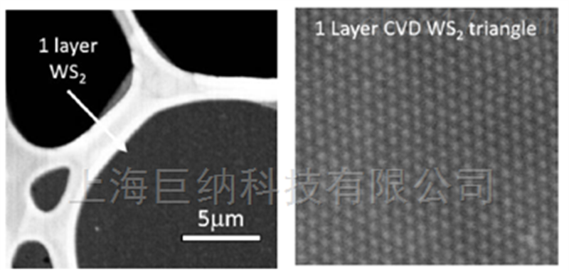
Transmission electron images (TEM) acquired from CVD grown full area coverage WS2 monolayers on c-cut sapphire confirming highly crystalline nature of monolayers
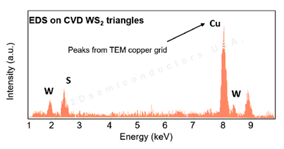
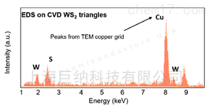
Energy dispersive X-ray spectroscopy (EDX) characterization on CVD grown full area coverage monolayer WS2 on c-cut sapphire confirming W:S 1:2 ratios
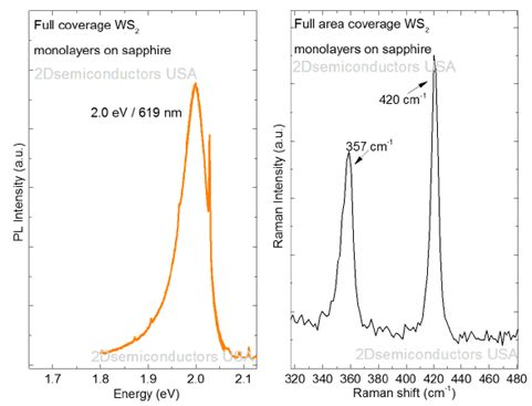
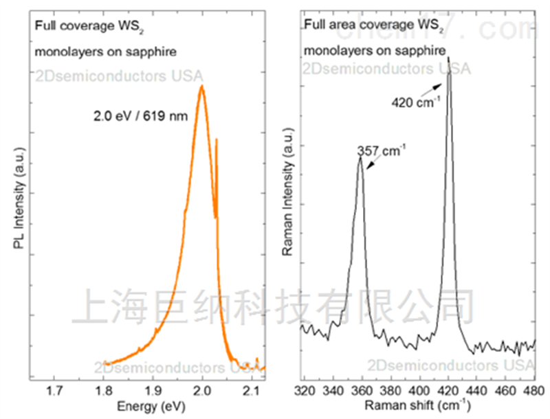
Room temperature photoluminescence spectroscopy (PL) and Raman spectroscopy (Raman) measurements performed on CVD grown full area coverage WS2 monolayers on c-cut sapphire. Raman spectroscopy measurement confirm monolayer nature of the CVD grown samples and PL spectrum display sharp and bright PL peak located at 2.00 eV in agreement with the literature.
産品咨詢
聯系我(wǒ)們
上海逅飛科技有限公司 公司地址:上海市虹口區寶山路778号海倫國際大(dà)廈5樓 技術支持:化工(gōng)儀器網掃一(yī)掃 更多精彩

微信二維碼

網站二維碼
微信掃一(yī)掃
