當前位置:首頁 > 産品中(zhōng)心 > 二維材料 > 硒化物(wù)晶體(tǐ) > SnSe 硒化錫晶體(tǐ) (Tin Selenide)


相關文章
Related Articles詳細介紹
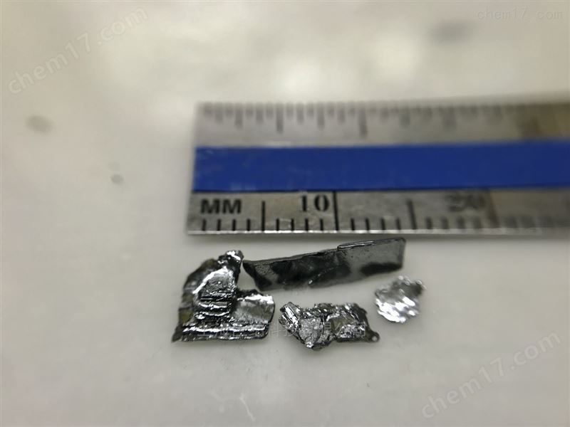
In the bulk form SnSe has band-gap at around 0.9 eV (indirect) and 1.25 direct gaps. It has layered structure (lamellar) with weak interlayer coupling, enabling to isolate down to monolayers. Each monolayer is four atoms thick (Se-Sn-Sn-Se) that is roughly 0.9-1.0 nm. At high pressures it undergo semiconductor to superconductor transition. More recently, SnSe has been shown to display world record performance for thermoelectric material efficiency.
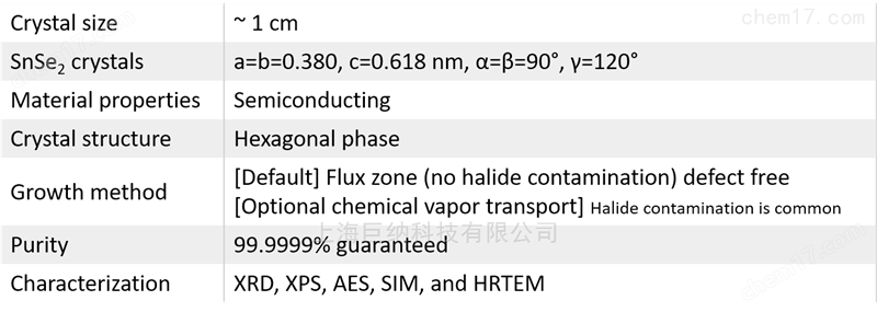
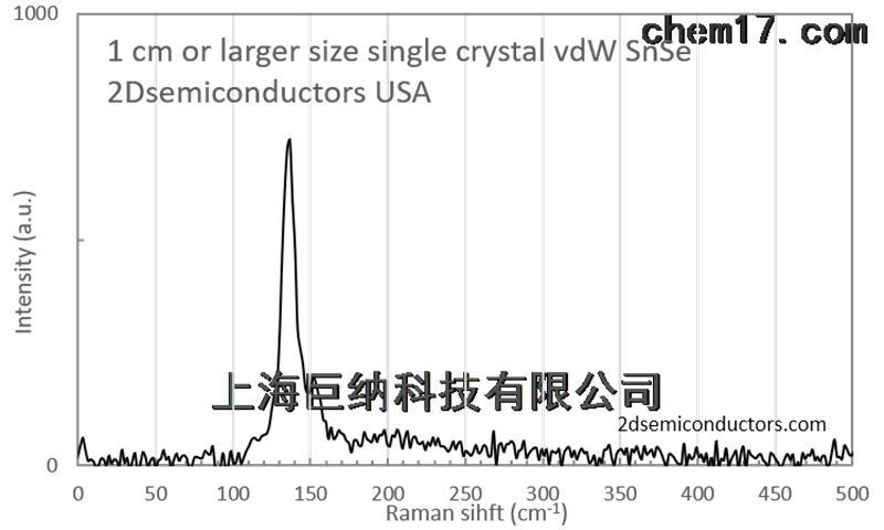
SnSe single crystal characteristics


産品咨詢
聯系我(wǒ)們
上海逅飛科技有限公司 公司地址:上海市虹口區寶山路778号海倫國際大(dà)廈5樓 技術支持:化工(gōng)儀器網掃一(yī)掃 更多精彩

微信二維碼

網站二維碼
微信掃一(yī)掃
